Beating the
chip part2
Before
emailing me please read this.
After a six year break there is more at nerdipedia.com
Part1 cracking the 2100p protocol
Part2 cracking the 1290 protocol
– This page was written before chip resetters were available for the (then) modern printers. Almost everyone visiting this site will be better off buying a resetter than trying to build one. Many people can simply use the free SSC service utility (see “Software only solutions” below). The rare exceptions are people who simply want to do it for fun, people who want to see or modify the chip data and people living in countries where resetters don't exist due to a trade embargo. I have considered pulling these page to stop the emails coming. After a few thousand “help me” messages I'm quite sick of them. I have other things to do - if you don't believe me look around the rest of the site.
21-may-03,I've had a couple of reports that lowering the value of the resistor(s) has been necessary to make it work. I presume some printer ports have a lower input impedance than mine – possibly due to resistive termination. The circuit at “ampoule” has been modified to put a transistor in the data path. Note that this will invert the signal so my program will not work with it. Modifying my code to do both shouldn't be too hard but I don't have time. I have put my project source online as JPL if anyone want to take it over.
24'th Mar 2003,
I'm still getting too many emails from novices asking for help. If you don't know basic electronics find someone to help you. I do not have time to diagnose faults by email. There is also a new site (it is not one of mine) that may be of help.
http://www.ampoule.ru/epson/en/index.html
10'th of November 2002,
In part one I used a micro controller to analyze the chip
signals and reset the ink chip. Building that sort of circuit is
beyond most people. Programming the code into the micro requires
a programmer (a device not a human) and some specialist
knowledge. If I were building a commercial chip reseter (which
I'm not) a micro is definitely the way to go.
But for the less
technically able I've come up with this circuit. Someone with
basic soldering skills should be able to knock it together.
For printer ports with 5
volt levels the circuit looks like this.
Some chips may
tolerate 5 volt and not need this, in particular 3'rd party chip.
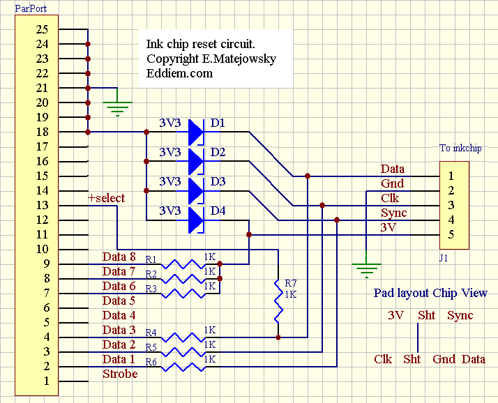
The circuit is for a printer port dongle. A
companion windows program will be available below (does anyone
want to port it to linux?). The circuit mainly consist of 3.3
volt clamps to convert the ports 5 volt levels to 3.3 volts. The
only tricky bit is the data line. When the chips data line is in
an input mode it is driven by port data line 3 via resistor R4.
When it switched to output mode the chip override the signal and
the output is sensed by the +select line. When the chip is
outputting data I pull data-3 high so it becomes a pullup to
3.3V
My printer port has no trouble reading the signal but
your mileage may vary.
The software is written in delphi 5 and requires a free DDL to work. Windows being windows I can't guarantee the program timing. I'm running the serial clock very slowly (1khz) but it seems to work fine. But if windows goes to sleep half way thru a chip write cycle I don't know what it will do to the chip – hopefully nothing bad but I don't know that yet.
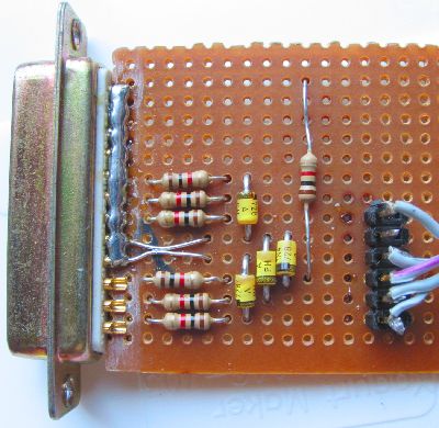
Bit
6 7 and 8 supply power to the inkchip, this is the upper group of
resisters and top zener.
The plug pins which are soldered
together are ground.
The odd vertical resistor routes the chip
data line to the +select input.
The pins in the strip on the
right are
3.3V power (top)
gnd
gnd
data
clk
sync(bottom)
Note that the DB25 pads are not at 0.1 inch spacing and the strips on the veriboard are - so only 4 pads are soldered and offending bit of strips are removed.
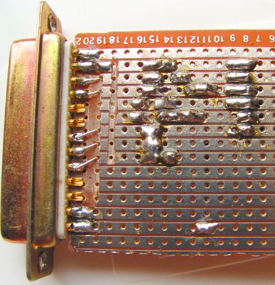
For printer ports with 3 volts levels things are even easier.
The
interface come down to one resistor. A few extra resistor could
be added to protect the port from short circuits.
Note that
all solder connections are on the upper row EXPECT black which is
on the bottom.
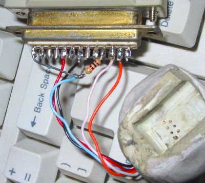
You can see my home brew chip socket here
also.
The wires are
orange = sync
white = clock
blue
= data
Black = ground
Red = power.
The program...
First - copy Fred Bulback's io.dll into the
directory you put my program in.
See:http://geekhideout.com/downloads/io.dll
My prog can be found here.
There is lots of stuff in the debug menu to help
you test the port etc – be careful with it when a chip is
attached.
If you are contemplating this project – start
by running this program. Disconnect anything you have on the
printer port and run
“Debug/make clock”, this
should produce a 10,000 cycle 1K clock and show you a message
when it is done. If this work it shows your computer timer is
compatible with my program (which uses queryperformancefrequency
and QueryPerformanceCounter).
There is a danger that leaving some port lines high and attaching a chip will do bad things. I will add a reset-port command soon.
Or you can try “debug/show freq” to display your counter frequency – if it shows zero you're out of luck – let me know if this happens.
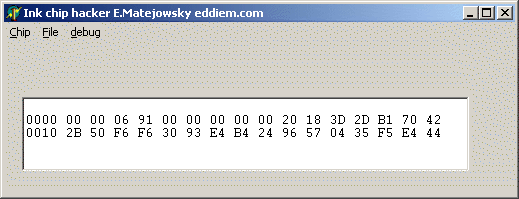
The chips have a 3 bit address/id. During the Read and Reset chip procedures my code tries all 8 possible addresses and displays the contents as seen in the graphic above. The first byte is the ink level, it is zeroed to make the chip “full” ie zero ink used. Someone with time to spare may wish to decode the rest.
I guess I should add a “write chip” command one day.
That's is for now, have fun and don't let the smoke out of the components.
Monday - 11'th
November.
Good news and bad news.
The bad is I've blown up several ink chips. I think
the reason may be bad contacts in the improvised chip socket I'm
using or from running them under voltage.
The good news is my
printer port uses 3.3 volts signals. I first thought is was
faulty but my notebook uses 3.3V as well. This means the above
circuit is not needed and a minimalist interface consists of one
resistor (R7). I've done it and it works.
Monday - 12'th
November Beta 1.2
Good news – I didn't blown up the chips. The
flaky socket had caused the chip to go into write mode and it was
filled with “ff”s. Not only were they erased but
there Ids had all changed to 7 (all address bits high). Looking
at the data I'd read out of the chips I noticed that 4 bits in
the last byte was always the same as the ID. I had speculated
that these bit might determine the id the chip responds to. I
haven't set out to test it but it sure looks that way now. I was
able to restore the chips data I'd saved to disk. I had to power
cycle the printer before it was happy but it is reading all the
chips again.
To restore the chips - I added two more commands
to the program. One is “blind reset” which pumps out
all the possible ink level reset codes without trying to find a
chip first. The other is “write chip” which finds the
chip ID and then programs the data from the programs buffer into
the chip. The buffer can be loaded from disk or another chip. The
data files are simple text files so they can be edited if need
be.
Sunday 1'st
December. Beta 1.21
Minor update, reads are now much
faster, this should reduce the number of chips which are
accidentally erased.
Monday 2'nd
December. Beta 1.3
3'rd party chips for the C60 (Jet
Tek) needed a delay after the last byte was written. This has
been added along with a C60 menu.
I think I've worked out the protocol for some of the other chips. The ones I used are from a 1290. These chips have the 2 centre pins on the row of 4 shorted out. I believe 870/875 etc also use them.
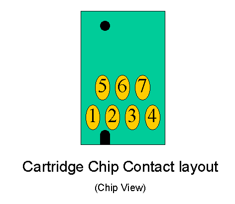
These use one extra signal (R/W). The pads are
-
1-data, 2+3 ground,4 R/W, 5 clk, 6 power, 7 sync.
My interface looks like this.

The
same as the 2100 except for the green wire.
The wires are
orange = sync
white
= clock
blue = data
Black = ground
Red = power.
GREEN
= R/W
I have run the chip at 5 volts without smoke and also on my 3.3 printer port interface.
I don't have a 1290 printer so this is unproven. I can read/write the chips and I'm fairly sure the first bytes are the ink level so it should work.
7600/9600 chips.
I can read
them but haven't tried to reset them yet, the ink level appears
to be stored in a different place to the other chip (I'm guessing
2'nd byte).
Monday
27'nd Jan 2003. Beta 1.4
Support for 1290 type chips
(870 etc)
I now know the epson names and numbers for the chips
( different from the ones I made up)
7600/9600 pad layout.
Epson numbering is
2 4 6
1 3 5 7
my names for the signals was
sync power data
gnd clock R/W gnd
Epson call them
csm pwrm o/im
com clockm r/wm gndm.
The you can read and write them using the 1290 menu but don't use reset.
Software only solutions.
I am aware of quite a few programs for resetting
the ink levels. Some are free and some are not. The program athttp://www.ssclg.com/epson.shtml
should be of interest to many visitors. I
have no connection with SSC Service Utility– don't send report files (testrep.txt) to me.
There
are also problems resetting completely empty carts on some
printers. This type of software can only work because epson have
left “back doors” or service modes in the printer
firmware. There is no guarantee future printers (even future
manufacturing runs of current models) will be able to work with
such software. As well as being able to reset ink levels the
above program offer manual control of the cleaning cycles –
this is something I really want to have.
December 2003,
I had hoped SSC would make this
page obsolete but sadly it does not work with my printer and
several people have written to me reporting the same. Some of the
features which worked on the version 2.91 are now broken on V3.1
– epson may well have closed the door to this type of
solution.
Sunday 1'st
December.2003 Beta 1.5
I've had many emails over the
last year or so saying “Does this program work with printer
epson XYZ, I can't get it to work”. My terse reply often
amounts to “How the @#$# would I know, I don't have printer
XYZ – buy resetter and quit bugging me”
Anyhow
today I tried to convert chips from a c82 (I think cart no TO323
etc ) to work in the 2100p and I couldn't write to them. I could
read them but writes would always result in $FF being written.
After much wasted time I found I had to slow the clock down to
write these. It will be interesting to see if the printer can
write to them (it can). The new version is online.
My
program.
Beta 1.5 is online
now
The project source code is here - This is written in Delphi-5.
A Unix port by By Benoy George.
George
has ported my code to a unix command line version. A massive 4K
source archive is mirrored here.
Eddie.M.